-40%
New J-Link OB ARM Debugger Programmer Downloader replace v8 SWD
$ 6.85
- Description
- Size Guide
Description
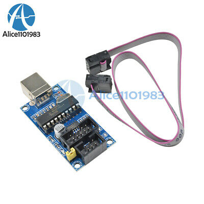
New J-Link OB ARM Debugger Programmer Downloader replace v8 SWDProduct Description:
J-Link- OB SEGGER developed by a separate set of emulator debugger downloader, generally designed to major companies Evaluation Board ("on-board"), which is the reason suffix "OB" of. The name "J-Link- OB" simulation download debugger with USB communication function, it can communicate with the PC, and the other end by SWD / JTAG mode and can support devices communicate, complete debugging Simulation debugging tasks.
We J-Link OB emulator debugger compared to the original J-Link OB fewer JTAG interface, leaving only the SWD interface to use ARM MCU core debug download many companies.
Supported object
All with SWD interface ARM7 \ 9 \ 11, Cortex-M0 \ M1 \ M2 \ M3 \ M4 \ A5 \ A8 \ A9 series of embedded microcontrollers.
Support generation MCU vendors are
:
ST, Freecale, nuvoton, NXP, TI,
Cypress, Atmel, Analog, Fujitsu, Toshiba
Energy Micro and so on.
Connection
: SWD mode
Supported IDE software
:
J-Flash ARM, Keil MDK-ARM, IAR EWARM, CoIDE, mikroC PRO for ARM, nRFgo Studio
Functionality, performance
:
Programming features: can be programmed FLASH ROM, EEPROM, AFR and the like.
Simulation capabilities: Supports full speed, single-step debugging, breakpoints, and other debugging method, you can view IO status, variable data.
Programming Performance: USB2.0 interface, perform SWD download, download speed is fast!
Simulation performance: USB2.0 interface simulation debugging, single stepping, breakpoints, fast response!
Product features:
1, simplify the interface, the use of the four line system: SWDIO, SWCLK, VCC, GND four interface, complete high-speed debugging, download.
2, fully compatible with the traditional J-Link, with J-Link all functions.
3, the use of USB Mirco interface (the current smart phone use), the data line.
4, 3.3V output, you can also give the target board power supply, easy user debugging and program download.
5, onboard recovery fuse, avoiding damage to the board circuit, more secure.
6, with a unique ID logo, multi device debugging is not conflict.
7, equipped with a transparent heat shrinkable tube, beautiful and more intimate protection.
8, work stability, without the phenomenon of the loss of firmware.
9, only U disk size, the circuit is simple, stable, reliable, easy to move and carry.
Package List
1 x J-Link OB
1 x USB cable
1 x Test line
Payment
* Only Paypal is accepted as payment.
* Must ship to a confirmed address, otherwise payment will be refunded and I will alert you to the cancellation.
* Immediate Payment is required.
Terms
* Returns are accepted only if the package has not been opened or damaged and the item is returned before 14 days or delivery.
* Buyer pays return shipping.
Feedback
My ability to succeed is up to offering the best customer service possible and earning top feedback and star ratings. Please contact me with any issue before leaving feedback and I will do everything possible to assure the optimal outcome.


